NO EXECUTE!
(c) 2011 by Darek Mihocka, founder, Emulators.com.
December 24 2011
2011 - The Year Of Smaller, Thinner, Faster
Steve Jobs may never stand on stage again to launch another product. Yet what he and Woz and other pioneers of technology developed over the past 35 years will continue to bring cool computing devices into our homes for years to come. Just think about that 35 year span. The Apple I launched in 1976 to hobby engineers for a price of $666 at a time when most of us watched television shows live (in black and white!), talked on a rotary telephone that was tethered to a kitchen wall, and wrote our reports on typewriters; electric if you were lucky. Apple I spawned Apple II which then spawned Commodore PET and C64, TRS-80, Atari 800, Acorn, IBM PC, Macintosh, laptops, Macbooks, and most recently tablets and cloud computing. Steve lived long enough to see 2011 be a watershed year in terms of "bang for the buck", performance, and size. Computer technologies such as microprocessors and flash made significant leaps in performance this year. Notebooks became smaller and thinner. And the technology I was waiting for last year - tablets - finally showed up in force in 2011. It is why I'm calling 2011 the "Year of Smaller, Thinner, Faster".
Before I start, full disclosure - I am still an Intel shareholder, as well as a shareholder in Amazon and Microsoft having worked as an engineer at all three of these companies. Their products are discussed in this posting.
Since my last postings in 2010 I have been jotting down ideas for topics and have categorized them today into these 5 categories:
- Sandy Bridge
- Bulldozer and AMD's real plan?
- Ivy Bridge and beyond
- Windows 7 / Windows 8
- Gadgets and Hardware
Feel free to use these links to skip ahead to ones you care about. Or, refill your egg nog and read this post all through before the Doctor Who premiere tomorrow night! As Christmas Eve winds to a close I for one am about to park myself on the couch for the next 24 hours to watch BBC America's marathon celebrating our Time Lord - the 11th Doctor Who. And as much as the planet, Mayan calendars, and humanity itself seem to be conspiring to send us back to the stone age by end of 2012, the world of science and technology continued to make great leaps and bounds in 2011. The gadgets I will discuss all cost under $1000 and many far less than that. Not bad considering the low value of our 2011 dollars compared to the relative value of what $666 was worth back in 1976.
The year of CPUs started with a bang barely a few days into 2011 at the Consumer Electronics Show with Intel's announcement of the "next generation Core", known by the codename Sandy Bridge:
Or if you're a CPU geek like me, you call it by its former name Gesher, in reference to the fact that it was designed at Intel Israel. A fine place which I got to visit a few years ago, employing some very clever engineers that I had the pleasure of working with. In fact many of the same people were behind the amazing Pentium M and Core 2 processors.
256-bit AVX
Sandy Bridge architecture adds significant new x86 register state visible to user mode applications. A wider set of 256-bit wide SIMD registers (now called YMM0 through YMM15) replace the older 128-bit XMM0-XMM15 registers used for SSE since 1999. The new instructions which operate on YMM registers are not called SSE5 as you might expect, but rather AVX, for Advanced Vector Extensions. And there are quite few instructions, with a solid 800 pages on new AVX documentation being posted by Intel.
http://software.intel.com/en-us/avx/
Adding new user mode register state is rarely done. Unlike x86 instruction set extensions - CPUID, CMPXCHG, MMX, AES, etc. - which simply add new operations to existing registers, adding new registers has consequences. Operating systems need to know about the new registers so as to properly context switch them when multi-tasking. Applications need to be recompiled or even re-written to make use of the new registers. Compilers and debuggers need to be updated. Virtual machine products - hypervisors, emulators, simulators, tracing runtimes - all need to be updated to support not just new instruction but new register state.
x86 register state has been extended very few times since the original 8086/8088 processors - x87 floating point was added, in 1986 most registers were widened from 16 bits to 32 bits to support future 32-bit operating systems such as NT and Linux, in 1999 the addition of the 128-bit wide XMM registers for SSE, and in 2003 for the 64-bit extensions. With MMX back in 1997 Intel even went out of their way to alias MMX state onto the x87 register just to avoid adding new state and breaking existing operating systems, but this trick created more problems than it solved. So in 2011 a huge block on register state was added for AVX.
Not surprisingly then, shortly after the Sandy Bridge processors started shipping, known by their Core i5/i7 2xxx brand names, a lot of software products were upgraded or patched to support AVX. Within months these products were some that were upgraded for AVX:
- Windows 7 and Windows 2008 R2 - Service Pack 1 added AVX support
- Visual Studio 2010 - Service Pack 1 added AVX support in compiler and debugger
- Xen - version 4.0 added AVX guest support
- Bochs 2.4.6 and 2.5 - added AVX AVX2 and BMI instruction simulation
- gcc 4.6 - improved AVX code generation, later then used by Fedora 15 and Fedora 16, Ubuntu 11.10
Unlike MMX and SSE which it replaces, AVX is designed to be forward compatible such that the true width of the SIMD registers need not always be known. As was done both in the 64-bit PowerPC extensions and AMD64 64-bit x86 extensions, many AVX operations are zero-extending and thus can operate on an arbitrary sized register width in the future. To help with context switching, the XSAVE and XRESTORE instruction were introduced which deprecate the older FNSAVE/FXSAVE mechanism which worked on fixed-sides register state. Operating systems such as Linux and Windows which use XSAVE will be more future-proof and not require these immediate patches as happened with AVX. Although of course obviously applications and compiler tools will still need to be upgraded to take advantage of any new instructions.
But it turns out Sandy Bridge is about a lot more than just new SIMD instructions to speed up your DVD ripping. Sandy Bridge is a "tock" as Intel calls it, one half of the "tick tock" product cycle they've used for a number of years now. A "tick" is a die shrink, a switch from say 90nm to 65nm technology. The 45nm Core 2 "Penryn" from 2007 and the 32nm Core i7 "Westmere" in 2010 were ticks. A "tock" is a significant change in micro-architecture using existing transistor technology. A tock allows Intel to improve on the design of the x86 pipeline. These redesigns are generally done to handle higher clock speeds and support new instructions, because how one designs a CPU pipeline to run at 1.6 GHz is entirely different and will have fewer stages than one that is designed to run at say 4 GHz.
I have confirmed now with several Sandy Bridge processors I've purchased that it overclocks significantly faster with ease. My one 2600K system is set to 103 MHz bus speed and 44x multiplier for a solid sustainable clock speed of 4.43 GHz that has been running like that for months now. That's a solid 50% faster clock than most of my existing 2.66 GHz Core 2 and Core i7 systems run at using same size L3 cache (8MB) L2 cache (256K) L1 caches (32K each) as previous Core i7 generation.
Higher IPC
The general rule of thumb with most CPU architectures is they can deliver one instruction per clock cycle, meaning an IPC rate of 1.0. The IPC on old 386 and 486 processor was slightly below 1.0 due to many instructions requiring multiple clock cycles and the fast that the pipeline was in-order so when an instruction stalled all instructions in the pipe stalled. Pentium 4 was signed to be high clock speed low-IPC and truly delivered a horrific IPC of 0.5 (meaning two clock cycles per instruction on average). AMD Opteron and Intel Core 2 brought IPC back up to about the 1.1 to 1.3 range and it has mostly stayed around there through Penryn, Nehalem, and Westmere variants of Core 2 and Core i5/i7. The low-power Atom processor found in many netbooks has an IPC rate similar to Pentium 4 at about 0.5, which is why at similar 1.6 GHz clock speeds an Atom is much slower than say a Core 2 based laptop.
Sandy Bridge I've found adds about an additional 15% performance at the same clock speed, meaning it can deliver an IPC above 1.5 for most code. Or in other words, a single thread of x86 code running on a 3.5 GHz Sandy Bridge processor runs at about the same performance as would require a 4.0 GHz Core 2 processor, or about a 10 GHz Pentium 4. Sandy Bridge delivers extra performance per clock cycle, and not simply due to the higher clock speed. 15% is about the minimum you will see, and some applications and benchmarks will show 20% or even 25% improvement.
Using my trusty old CPU_TEST utility from many past postings, I ran it on my Core i7 2600K processor to find out what changed. Just as you the reader can by the way, see my old postings from 2008 for directions on how to run it.
As you may recall back in 2008 I was unimpressed by the Core i7 "Nehalem" architecture, because for most x86 instructions it had the same timing as Core 2. IPC didn't really change. yes, it added L3 cache, it brought back Hyper-Threading, but it also increased L1 cache latency from 3 cycles to 4 cycles, hurting performance of heavily memory indirection based code such as found in simulators and emulators. And so even as I worked at Intel in 2009 and 2010 I insisted they give me a Core 2 workstation, not Core i7, for my simulation work.
Sandy Bridge is a true improvement. L1 cache latency is still 4 cycles, but one of the major enhancements in the architecture is the addition of a second load port, which means it can execute up to two memory load instructions per clock cycle, not one. AMD has had this advantage for a long time and now Sandy Bridge matches that, allowing the out-of-order execution core more freedom to speculatively issue memory loads than in Core 2 or previous Core i7.
For when a memory access misses the L1 or L2 cache, in Core 2 you would then have to go to main memory at a cost of about 300 clock cycles. Nehalem (and Westmere) Core i7 architectures introduced an L3 cache of 8 to 12 megabytes to act as yet another buffer layer. Due to the size and distance on the die from the core, accesses to L3 cost about 45 to 50 clock cycles by my measurements back in 2008 and 2009. Sandy Bridge reduces L3 cache latency to about 35 cycles from what I measure today on the same 8 megabyte L3 cache size as before. That means that programs with a fairly small working set (in the single digit megabytes) will hit L3 cache much faster than before and rarely need to touch memory.
Measuring the micro-architectural improvements
But the key reason that Sandy Bridge is faster is that plain old integer arithmetic and load operations now parallelize better, what's called ILP or "instruction level parallelism". Almost any CPU, whether Intel, AMD, PowerPC, ARM, 68040, etc. can execute say one integer addition per clock cycle. It's because a modern ALU is designed to process one new arithmetic operation per cycle. Pentium 4 had the concept of "double pumped ALU" which could perform two additions per cycle by running internally at twice the clock speed. That unfortunately did not scale well with higher clock speeds. So most cores today instead use multiple ALUs in parallel to execute multiple additions per clock cycle. Core i7 Nehalem for example can perform two integer additions per cycle. Sandy Bridge can do three. Nehalem can perform one simple LEA instruction per cycle (simple LEA being an instruction that can be used to perform addition or certain subset of multiply) while Sandy Bridge can do two per cycle.
Why does this matter? Arithmetics like ADD and SUB and LEA are very common operations in x86, so if you can improve the parallelism of those, the more efficient the out-of-order core can be.
There is another subtle change in Sandy Bridge that most people will never notice, and that's the much improved partial-register EFLAGS handling. This was one of the Achilles heels of Pentium 4 and problematic every since the Pentium Pro and Pentium II days. Any time you wanted to update part of EFLAGS, or even read EFLAGS register, it cost you a lot of cycles. There is an infamous code sequence I've mentioned before consisting of an ADC (add with carry) followed by an increment or decrement instruction (INC or DEC). It appears in things like multi-precision arithmetic code where ADC instructions are used to propagate the carry-out of each addition into the next, and wrap the ADC instructions in a loop controlled by INC or DEC to count the number of iterations. Intel designed the INC and DEC instructions 30 years ago to not muck with the Carry Flag for just this scenario, yet there is a huge problem. ADC followed by INC or DEC causes the arithmetic bits in the EFLAGS register to be split across two instructions and have to be merged in microcode, which stalls the pipeline. Everything from Pentium II to Pentium 4 and Core 2 and previous Core i7 suffer from this. Sandy Bridge eliminates that stall. ADC INC now executes five times faster than before.
Reading the EFLAGS register is also much faster thanks to improvements in the latency of LAHF and PUSHF instructions. Reading EFLAGS is an operation is useful to many emulators and instrumentation frameworks such as PIN or DynamoRIO,
Additions, memory loads, reading the flags, cache latency, zeroing memory - these are all very fundamental operations in just about any piece of code and therefore why I pay so much attention to their cycle counts. If you look at the CPU_TEST output of these specific tests that I list below, it is clear that Sandy Bridge designers focused on improving the fundamental throughput of basic x86 operations, leading to the much higher IPC than previous processors.
| Test | Nehalem cycles | Sandy Bridge cycles | Comments |
| test 1 int add | 1.0 | 1.0 | sequential data dependent ADD instructions |
| test 1 int adc | 2.0 | 2.0 | sequential data dependent ADC instructions |
| test 1 lea smpl | 1.0 | 1.0 | sequential data dependent LEA instructions |
| test 1 lea cmplx | 1.0 | 3.0 | sequential data dependent complex LEA reg1,reg2+reg3*scale+disp |
| test 1 mem load | 1.0 | 0.5 | memory loads without data dependency |
| test 1 mem indir | 4.0 | 4.0 | memory loads doing "pointer chasing" |
| test 2 int add | 1.0 | 0.5 | tests pairs of mutually exclusive adds |
| test 2 int adc++ | 5.0 | 1.0 | tests pairs of mutually exclusive ADC / INC instructions |
| test 3 int add | 0.5 | 0.33 | tests triplets of mutually exclusive ADD operations |
| test 3 lea smpl | 1.0 | 0.5 | triplets of simple LEA operations |
| test 3 lea cmplx | 1.0 | 1.0 | triplets of LEA reg1,reg2+reg3*scale+disp |
| test 4 int add | 0.5 | 0.33 | four mutually exclusive adds |
| test 5 zero mem | 1.6 | 1.0 | store of zero immediate to memory |
| test 13 pshf/pop | 15.5 | 2.0 | PUSHFD POP reg, a common way to read EFLAGS |
| test 14 inc/lahf | 10.0 | 2.0 | INC LAHF, measures LAHF latency |
| mem random 2048K | 44 | 35 | memory latency of L3 cache using 4MB block |
As an example of how these improvements benefit real code, I tested with a very branchy and memory intensive application like Bochs. I compiled Bochs 2.5 using Visual Studio 2011 preview edition (more on that later), and booted Windows XP guest OS with my usual set of benchmarks. My T1FAST and T1SLOW integer benchmarks emulate at a rate of 100 to 110 MIPS on the reference 2.66 GHz Core 2 machine I've done my measurements in past Bochs benchmark runs. Run on my Sandy Bridge Core i7 2600K overclocked to 4.43 GHz, I get 190 to 210 MIPS for the exact same test code running on the exact same Bochs binary. That's is about a 90% speedup of Sandy Bridge over Core 2 overall. Yet clock speed scaling (4.43 GHz to 2.66 GHz) alone would only give a 66% speedup, since 4.43/2.66 = 1.66. The remained is the gain from micro-architectural improvements in Sandy Bridge, which gives us 1.9/1.66 = 1.15 gain, or in other words, 15% higher IPC. And that's not even taking advantage of AVX.
Lower power consumption notebooks
When you can get 15% faster performance at the same clock speed, conversely that means you can reduce clock speed about 13% to get the same performance as older processors. Instead of clocking a laptop at 1.8 GHz using older Core i7, you can now clock it at 1.6 GHz to get the same level of performance. This is exactly what we saw happen in July of this year, with the introduction of Intel's 17 watt Sandy Bridge part and notebooks such as the latest Macbook Air and ASUS Ultrabook that use it. Lower power consumption means smaller fans, smaller heat sinks, smaller products.
Let us not forget AMD. After many years of hype about "Bulldozer", their latest x86 micro-architecture, AMD finally started to trickle out Bulldozer parts in October. They are improvements over past AMD Opteron and Phenom parts but not so much to impress. Bulldozer was largely slammed by the media, such as this review.
Bulldozer sounded great on paper. It runs at speeds well above 3 GHz, on par with Sandy Bridge parts. It now supports SSE4.1, SSE4.2, AES, CLMUL, and AVX extensions, which is huge news as far as instruction set compatibility with Intel. All prior AMD parts were only compatible up to SSE3 (Pentium 4), not even supporting the instruction sets of the Core 2 or Atom!!! Bulldozer and Sandy Bridge are effectively at the same level of x86 instruction compatibility.
So yes, on the positive side, Bulldozer is a Sandy Bridge clone that runs at Sandy Bridge clock speeds and sells for roughly Sandy Bridge prices. If you must buy AMD, knock yourself out choosing Bulldozer over some earlier AMD product. But, running at the same clock speed and delivering the same performance are two entirely different things. You will simply not get Sandy Bridge's level of performance out of Bulldozer. And I know why.
While other web sites have gone into detailed benchmark runs and explanations of why Bulldozer is a fail in performance, I only needed my CPU_TEST utility to see in a matter of seconds why it would fail. My friend Steven Noonan got his hands on one in October and ran the CPU_TEST program for me. The results confirm that Bulldozer continues AMD's design of having two load ports to issue two memory loads per cycle, and it continues AMD design of not having EFLAGS partial-register stalls. That's the good news.
But Sandy Bridge has addressed the load port and partial EFLAGS stalls now, and it is on other design details that Bulldozer loses and loses big:
- Bulldozer now has the same 4-cycle L1 cache latency as all the Core i5/i7 products. No longer the advantage of a 3-cycle L1 latency.
- Bulldozer is now slower than Sandy Bridge at PUSHFD and LAHF arithmetic flags instructions, so again, no longer an advantage.
- Bulldozer maxes out at 2 addition operations per cycle, compared to 3 in Sandy Bridge, meaning lower ILP on fundamental ALU operations.
- Bulldozer still uses an older style integer divider, needing 44 cycles to perform an integer addition instead of 22 cycle. Similarly, Bulldozer needs 4 cycles for integer multiply instead of 3. Therefore integer scaling operations are slower than Sandy Bridge.
- Bulldozer, as with previous AMD products, is consistently slower at most MMX and SSE operations. For example, a simple register move between 64-bit GPR and XMM (MOVD instruction) is 9 cycles instead of 1 on Sandy Bridge. This limits the ability to use SIMD registers as extensions of the integer register file.
- A very key instruction introduced in SSSE3 - byte permute (PSHUFB) - is 3 cycles instead of 1 cycle. Practically throw darts at any other SSE instructions, they mostly tend to be slower.
- L2 cache latency is almost twice as slow as Intel parts, looks like about 21 or 22 cycles as opposed to about 12 on Sandy Bridge.
- L3 cache latency appears to be about 44 cycles, comparable to older Intel parts but slower than Sandy Bridge's 35.
- Executing self-modifying code, and thus dynamic generation of code in Java or .NET, appears to be about twice as slow as Sandy Bridge.
- CMPXCHG, a fundamental atomic instruction using for synchronization primitives and locks appears to need about 50 cycles for an uncontended operation, more than twice as slow as Sandy Bridge.
Bulldozer exhibits lower ILP, slower EFLAGS operations, slower L2 and L3 cache latency, slower multiply and divide, slower MMX, slower SSE, slower dynamic code, slower locks. When you have so many significantly slower numbers in so many of the x86 micro-benchmarks it is almost certain you will get much lower IPC than Sandy Bridge on a given piece of x86 code. And that is the data that the benchmark sites reported to you back in October, minus the analysis I just gave you to explain why.
Now, AMD was sort of prepared for this, so they tend to emphasize not the poor single-threaded IPC performance but rather the overall throughput of the "8 cores" on the Bulldozer chip. I find their claim to be misleading, as it is based on confusing definitions of what a "core" is versus a "thread". Bulldozer is NOT an 8-core processor. It has 8 threads of execution running on 4 cores, similar to any Intel Core i7 part with 4 cores and 8 hyper-threads. Yet AMD tells people to think of it as an 8-core processor, and so Windows 7 does.
The result is AMD ended up with the snafu of even slower benchmark results due to operating systems such as Windows treating the 8 threads as 8 cores. The recent Microsoft Windows scheduling patch which attempts to improve thread scheduling on Bulldozer by treating as in fact as 4-core hyper-threaded processor exposed AMD's misleading marketing:
This kind of deception was completely unnecessary. If AMD simply said Bulldozer was quad-core with SMT (to avoid using Intel's term "hyper-thread"), everybody would have understood what that is and accepted it for what it is. But they got busted and their processor simply doesn't live up to the performance of a true 8-core AVX processor. Instead, AMD's marketing department chose to misuse the term "core" to mean "thread", and "module" to mean "core".
AMD's secret plan for the future: a Transmeta-style 64-bit do-over?
Call me a conspiracy theorist, but several things that AMD did this year lead me to believe that they're willing to surrender the x86 performance lead. I believe based on what I've seen this year that AMD is planning to get out of the x86 hardware business.
First of course is the evidence above that they didn't really try with Bulldozer. There are no significant architectural improvements to improve IPC anywhere near like what Intel did going from Pentium 4 to Core 2, or Nehalem to Sandy Bridge. They added SSE4 and AVX and added hyper-threading. They simply cloned a Core i7, and poorly. What this tells me is that not much engineering R&D effort is going into their x86 core design.
Second, in June they along with nVidia pulled out of the BAPCo, a consortium of companies that has jointly produced the well known SYSmark benchmark suite. SYSmark is a collection of "real world" applications, not micro-benchmarks, and is intended to show how well real code that real people run performs, code such as Microsoft Office applications, Flash, Photoshop, etc. AMD wouldn't pull out of something like this if it didn't serve their marketing needs. So one can deduce that they don't expect to be able to compete well in these benchmarks which, in the case of Microsoft Office, are mostly single-threaded integer applications.
http://www.anandtech.com/show/4464/amd-resigns-from-bapco-over-sysmark12-concerns
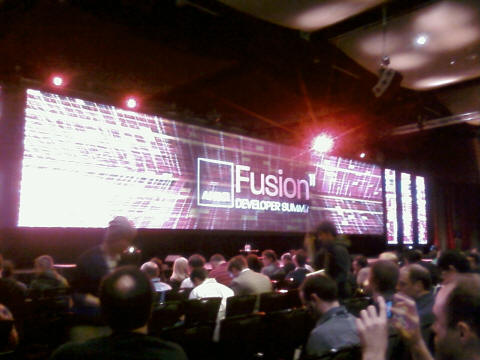
Third, that same month at a huge developer event held near Seattle, the AMD Fusion 11 Developer Summit, they went one come interesting new tangents and ARM and new core design.
http://developer.amd.com/afds/pages/2011_Highlights.aspx
http://developer.amd.com/afds/pages/keynote.aspx
One of their keynotes they brought an ARM VP to give this presentation on their partnership with AMD to push for open standards and push for lower power consumption:
http://developer.amd.com/afds/assets/keynotes/Compute_Power_with_Energy-Efficiency_Jem_AMD_v1.1.pdf
I went to that talk and was thinking ARM, really, ARM? AMD and ARM in bed? Apparently so, pushing for "open standards" and mentioning OpenCL a few times as an obvious slam against nVidia and CUDA. So AMD and ARM are pushing for OpenCL, which is of course used by graphics and HPC style applications, not single-threaded code.
Next clue, the first keynote of the conference, they announced the launch of the Llano processor. For a brief nanosecond I thought this was the launch of Bulldozer. Nope, Llano was based on same old SSE3 core they've been shipping before. The marketing emhpasis on Llano was on the GPU side of the chip, so again, diverting attention away from x86 performance.
The pieces started to fall together when I went to the AMD disclosure of a new GPU design they call AMD CORE NEXT. After how many years since acquiring ATI, AMD is retiring not only the Radeon brand name but also retiring ATI's VLIW-based GPU architecture. They are developing a new core architecture from scratch, as explained in these two presentations:
http://developer.amd.com/afds/assets/keynotes/6-Demers-FINAL.pdf
http://developer.amd.com/afds/assets/presentations/2620_final.pdf
As AMD explained, the VLIW design was difficult to generate efficient code for (ask anyone that's every tried programming the Itanium!), difficult for programmers to understand, difficult to debug. So they're killing it (good!). AMD is designing a new core which they call a GPU, but as you see in the slides they call the cores "Compute Units" not "shaders", which to me hints at non-graphical applications.
If you particularly look at the former PDF file, the 2620_final.pdf document, starting at about page 15 through page 25, they show what the instruction set of this new GPU looks like. Look familiar? To me it sure looks a lot like a RISC instruction set like Alpha or PowerPC. In fact notice that all of their instruction encodings are either 4-byte or 8-byte long encodings. No super wide VLIW like encodings, no arbitrary sized x86 encodings, just very straightforward RISC-like instructions with one destination two sources, or one destination three sources.
They kept emphasizing "a pointer is a pointer", meaning that a 64-bit pointer on the x86 core can be shared directly with this new core. Currently, whether on AMD processors or Intel processors or nVIDIA processors, memory mapping between x86 and GPU is different. A logical address that x86 code sees does not map to the same address that the GPU sees. nVIDIA's CUDA 4.0 introduced the concept of pointers to shared memory, but this is hack pulled off by pre-allocating identical ranges of address space both on the x86 side and GPU side. You still cannot take any arbitrary pointer to x86 memory and pass it to the GPU. AMD is claiming their new core does support that, that "a pointer is a pointer", along with full exception support, virtual memory and page tables, calls and conditional branches, integer operations with 256 GPRs, multi-threading, even atomic operations.
This is no GPU core. What AMD is describing here is a fully functional 64-bit CPU core that just happens to have a lot of SIMD juice support. This processor in theory could boot Linux given the integer functionality it appears to have.
Here is where it gets even more interesting...
AMD then disclosed that this instruction set they just showed is not the native hardware's instruction set, but close. This instruction set is really a virtual instruction set meant to be generated by compilers which then can target either an x86 CPU core or one of the new GPU cores using a dynamic jitter. The idea being that you the programmer don't write separate CPU code and GPU code, you just write code, and the system decides which kind of code to dynamically jit.
As I was sitting through these presentation and trying to decipher what AMD is really up to, this is what started brewing in my head:
- This new Core Next is not a GPU core, the name doesn't even imply graphics. Since this is a fully functional 64-bit integer core as well, why would AMD bother to duplicate such common functionality on the die with both x86 cores and Core Next cores? One obvious possibility is that AMD would eventually eliminate the hardware x86 core from the chip and have emulation software that translates x86 code to Core Next.
- Emulating x86 in a production processor is based in tried and tested technology that was developed over a decade ago - for example, Transmeta processors. Transmeta developed processors in the late 1990's which emulated x86 using a much simple instruction set, resulting in much lower power consumption and die size. Exactly what you'd want to do if you were trying to pack hundreds of low-power cores on a die, as the ARM keynote hinted at. Similar software emulation called IA32el was successfully used by Intel to emulate x86 on Itanium. China's Godson 3 processor uses a low-power MIPS core to emulate x86.
- This would explain the partnership with ARM. If there was a single common binary instruction set (Core Next) and common API (OpenCL) that applications were compiled to (as opposed today where you have PowerPC binaries, x86 binaries, 64-bit x64 binaries, ARM binaries, Cuda, DirectX, OpenMP, MPI, etc.) it would make it easy to write apps which scaled from the smaller ARM devices to the largest AMD servers and workstations. The instruction set is virtual, a translator would jit it to the actual target processor, just like with Java. The approach is even x86 compatible for existing hardware, since you could jit the Core Next instructions to x86 in much the way that Transitive's Rosetta allowed Apple emulate PowerPC RISC code on x86.
- Through this series of blog postings over the past 4+ years I have argued the case to punt x86 hardware in favour of efficient techniques implementing software emulation of x86 on non-x86 hardware.
Those of you who are regular readers will recall my two-part posting back in 2007 proposing punting x86 in favor of a new encoding which I called VX64 (Virtual eXecution 64) to be the basis of a new 64-bit instruction set. Gone are REX prefixes and 15-byte long instructions. VX64 would use 4-byte and 8-byte encodings to make it easy to encode for jit, and also easy to decode for hardware or another jit, and could easily accommodate opcode encodings for all of the existing x86 instruction set:
http://www.emulators.com/docs/nx05_vx64.htm
http://www.emulators.com/docs/nx06_rmw.htm
I was just brainstorming out loud about how to fix x86 in 2007 when I did my research and came up with these VX64 postings. It would not be a huge leap of the imagination to presume that AMD similarly had thoughts down the same path, or was even inspired by my posting. To summarize, and I have absolutely NO confirmation from anyone at AMD that this is what they're planning, but this is what I think AMD is really up to: you're AMD, you're getting your clock cleaned by Intel at peak x86 performance, so you stop on x86 design, pull out of the x86-centric benchmark consortium, deflect attention to multi-core throughput computing and graphics, focus your engineering on designing a ransmeta-style core that you initially market as a GPU core but secretly develop to be a fully-standalone CPU, develop a jitter or some kind of translator that would give you adequate x86 backward compatibility (like IA32el, like Rosetta), and partner up with companies like ARM to license your new ISA to to kill off both x86 and CUDA in one fell swoop.
Am I right?
AMD's Fusion event was held in June. In September I flew down to San Francisco to attend Intel's counterpart, the 2011 Intel Developer Forum at the Moscone Center. Obviously there was a lot of focus on Sandy Bridge. There was the announcement by Google during the keynote that they would now be "optimizing Android for x86" (I guess as opposed to before, just poorly porting it?). There was a very cool demo of a solar powered x86 CPU, which was powered by a single solar cell picking up the room light and then powering a Windows 7 machine running a video animation. As a light bulb was brought closer to the solar cell the Windows animation sped up. Neat trick, but no details on what the actual x86 core being demoed was other than I saw in the Task Manager briefly that there was 2 GB of RAM on the system and a single core.
Intel was giving a lot of detail about next year's Ivy Bridge processor, the 22nm die shrink (and therefore "tick") of Sandy Bridge. The processor is only a few months away and part numbers and prices are already posted online. In other words, no multi-year wait for Ivy Bridge as was the case for Bulldozer.
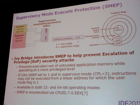
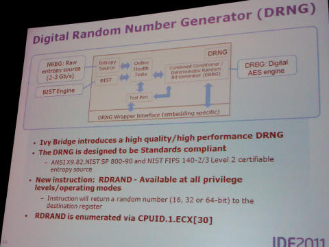
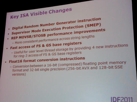
Being a "tick", Ivy Bridge does not add many new instructions over Sandy Bridge. One new feature called SMEP is interesting to kernel developers in that it can block access to user mode pages from kernel mode. I'm not terribly keen on this, as much like the No Execute / Execute Disable bit added a decade ago, this is a band aid solution to the problem of buggy exploitable code in Windows and Linux. It is a solution to a problem that could have been solved entirely in software to begin with.
A more interesting new feature is the random number generator, a way for code to get a purely random number each time it executes the RDRAND instruction.
What will be great for compiler writers and more so even for jitters are the new improvements to REP MOVSB and REP STOSB. These are the x86 instructions generally used to implement the C memcpy() and memset() functions and have been around since the original days of the 8086/8088. Over they years these instructions have gotten relatively slow and programmers are forced to roll their own memory copy loops using a combination of loop unrolling, and combinations of REP MOVSD and REP MOVSB instructions. And similarly for memory fills, same kind of contortions with REP STOSD and REP STOSB. As I understand it from the presentation, this will no longer be required. REP MOVSB will just copy memory as expected, and do so efficiently. REP STOSB will fill memory efficiently. As it should have always been.
The big claim relevant to us all about Ivy Bridge is that it has half the power consumption of Sandy Bridge while delivering the same throughput as Sandy Bridge. Apparently the shrink in transistor size from what they call 32nm "planar transistors" to 22nm "3-D transistors" truly cuts power consumption by 50% in one generation. This has huge ramifications for notebook computers and tablets in terms of battery life, and for servers in terms of cooling and rack density. We'll see when the final product comes out but initial indications are that the Ivy Bridge processors will max out at 77 watts, lower that today's 95 watt Sandy Bridge desktop parts.
Is the netbook dead?
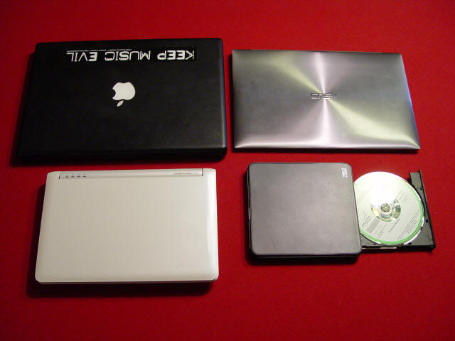
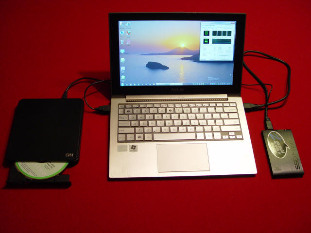
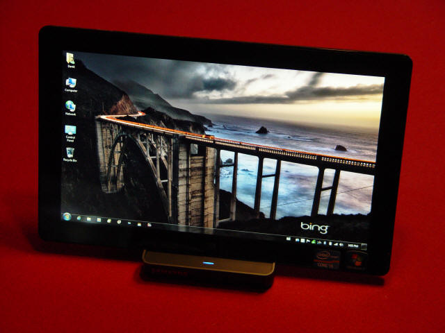
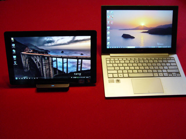
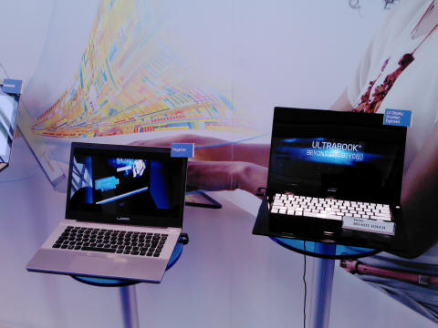
There was a lot of talk about Ultrabooks, sleek thin notebook computers modeled after the Macbook Air and similarly powered not by Atom but by big cores like Sandy Bridge and Ivy Bridge. If you look closely at one of these two demo Ultrabooks in this photo, quite possibly the slogan "Beyond The Beyond" is the most idiotic marketing slogan I've ever seen. Ignoring the stupid slogan, the Ultrabooks are neat and I will show one up close in the Gadgets section.
Intel also discussed their post-Ivy Bridge processor codenamed Haswell which they claimed would bring all-day computing to notebook computers. If that is true, the Atom netbook is practically dead in a year or two. Haswell would be the 22nm "tock", meaning major feature upgrades. So possibly more IPC increases leading to lower clock speeds and lower power consumption. The current lowest wattage Sandy Bridge that is found in the Macbook Air and Ultrabooks consumes 17 watts. Cut that in half for Ivy Bridge and possibly more in Haswell and that brings it into the single digit power consumption range of Atom but triple the performance.
New 22nm instruction extensions
Long before IDF (which was in September), in fact shortly after the AMD Fusion 11 Summit here in Seattle in June, Intel made a surprising move and posted online updates to their x86 ISA manuals that cover not only Sandy Bridge and AVX, but also new instruction extensions which will appear in 22nm processors such as AVX2 and BMI (Bit Manipulation Instructions). Since Ivy Bridge only adds a handful of new instructions, these presumably then appear in Haswell or later.
If you want a peek into this (far?) future of Intel's ISA, you can follow along by downloading the latest manuals from this documentation page:
http://www.intel.com/content/www/us/en/processors/architectures-software-developer-manuals.html
I recommend downloading the huge single PDF that contains all three sets of volumes in about 4000 pages. Much easier to read and search through that multiple PDF files. I also recommend downloading the separate AVX manual which discusses AVX2, and BMI in more detail. That document is currently at: http://software.intel.com/file/36945 or can be found linked to on that main documentation page.
The BMI set of instructions that I am keen on are what they call the VEX-Encoded GPR Instructions, described in Chapter 7 of the AVX manual. These are technically AVX instructions encoded using the AVX instruction forms, but they operate not on SIMD state but on plain old integer general purpose registers (the GPRs). It is a set of 16 instructions when I saw them I immediately thought of uses in simulation and emulation that would improve IPC.
One of the new features of the encodings used with AVX is that they support non-destructive destination registers. This means that instead of encoding an instruction in this two-operand form:
ADD regDest, regSrc
where the destination register is also one of the inputs, AVX allows for write-only destination registers, where an instruction has a three-operand form like this:
ADD regDest, regSrc1, regSrc2
This is very RISC-like of course, and serves to improve instruction parallelism by eliminating the need to copy a source operand into a destination register first. If you write x86 assembly, think of all the extra MOV instructions you frequently emit just to shuffle data around in registers.
Old Mac and Atari programmers may grimace at the thought since what I'm about to describe existing in both the PowerPC but also the 68020/68030. In over 30 years the x86 instruction set has never implemented a bitfield extraction instruction. i.e. give me some data and I'd like to extract 3 bits from bit position 5. Exactly the kind of thing compression and encryption code does a lot, or simulators do when decoding instructions. 68020 had BFEXT, PowerPC had RLWINM, and now finally x86 will have the BEXTR instruction and works exactly how you've been waiting for it to work.
The MULX instruction is a form of multiply which does not update EFLAGS at all. Recall that today in x86, multiply, divide, shift, and rotate all have funky "undefined" EFLAGS outputs. This leads to the EFLAGS partial-register stalls I discussed earlier, and leads to false data dependencies on EFLAGS which then leads to lower ILP and lower IPC. MULX is a three-operand non-destructive multiply that does not EFLAGS. Similarly there are three-operand forms of shifts and rotates that do not touch EFLAGS, called SARX SHLX SHRX and RORX respectively.
The most interesting new instructions that I am looking forward to are PEXT (Parallel Extract) and PDEP (Parallel Deposit). These are a new class of bitfield manipulation instructions that can be used for shifts as well as for extracting from or setting (depositing) into multiple bitfields at once. The best way to picture them is to think about the powerful PowerPC RLWINM and RLWIMI instructions, which perform single bitfield extract and deposit. On PowerPC you specify a source register that contains bits to manipulate and three more input values which specify a shift count, the starting bit, and ending bit positions of the bitfield. By setting those three values appropriately you can perform a bitfield extract or insertion, a rotate left, a rotate right, a shift left, or a shift right.
Now imagine if instead of { shift count, start bit, end bit } you provided a bitmask in a second source register. This bitmask can contain arbitrary bits, which tell the instructions where one or more bitfields are located. Using a sequence of PEXT and PDEP instructions you could for example perform arithmetic operations on a packed bitfields without the usual slow sequence of multiple shifts and masks and related EFLAGS dependencies.
Another explanation of how parallel extract and deposit work, as well as how one designs such as shifter in hardware, can be found in this IEEE paper originally written in 2007:
http://palms.princeton.edu/system/files/IEEE_TC09_NewBasisForShifters.pdf
Bochs 2.5 and new simulation papers
While these new 22nm instructions are obviously not available in hardware today, you can experiment with them by running AVX2 abd BMI test code today. The Bochs 2.5 simulator was just released a month ago at the usual http://bochs.sourceforge.net/ site and supports simulation of these 22nm instruction extensions including AVX2 and BMI. If it is documented in the Intel ISA manual, it is already implemented in Bochs 2.5!
Bochs 2.5 has all sorts of other new features, including the ability to select CPU features without recompiling. No longer do you need to recompile Bochs to say, add 64-bit mode support, or remove SSE support. Most CPU features from x87 to MMX to SSE to AVX and 64-bit mode are now always compiled into the Bochs binary and can be dynamically enabled and disabled from within the bochsrc.txt file.
Bochs 2.5 also has two optimizations based on my past postings regarding lazy flags evaluation (Part 11) and using handler chaining to improve the branch prediction rate (Part 25) which deliver up to about 10% performance increase over Bochs 2.4.x.
In fact, 2011 was a great year in the field of simulation, with not only the Bochs 2.5 release making it an even better gold standard x86 simulator but also with the publication of a couple of papers by Intel. The first paper I'm referring to came out this spring at the 2011 CGO (Code Generation and Optimization) conference WISH workshop and describes Intel's ZSIM simulator for tracing through x86 or other instruction sets using a combination of lazy flags, interpretation, and jitting techniques.
http://www.cs.virginia.edu/kim/docs/wish11zsim.pdf
The second paper is one I co-wrote with my Intel colleagues last year and got published this year at the 2011 ISCA conference workshop known as AMAS-BT. That is the same workshop where in Beijing in 2008 Stanislav and I presented our first paper on fast interpretation techniques in Bochs. This year's paper discussed a simulator I worked on internally at Intel in 2009 and 2010 to model not just x86 but rather the low-level microcode that x86 decomposes into inside of the pipeline. This is more tricky than simply emulating 68040 or PowerPC or x86, since microcode can issue multiple instructions in the same clock cycle and so you have to atomically simulate multiple instructions retiring at the same time. Using very much the same techniques shared by Bochs and ZSIM, and writing the simulator from scratch in C++ with the goal of tuning it for Intel's current micro-architectures, my co-author Jens and I managed to reach simulation speeds exceeding 200 million micro-ops per cycle. Which is great, considering the simulator it replaced was about 20 times slower!
http://amas-bt.cs.virginia.edu/2011proceedings/amasbt2011-p3.pdf
If you work on any kind of interpreter, simulator, or even a jitter, and you haven't tuned the code recently I would urge you to give these a read.
Returning back to the IDF conference, September 13 2011 was a major day for developers. It was not only day 1 of the Intel's Developer Forum in San Francisco, it was also day 1 of Microsoft's developer conference known as MS BUILD, held 400 miles south in Los Angeles. I was sitting at the keynote watching Intel CEO Paul Otellini deliver his keynote with the solar powered x86 processor and talking about Ivy Bridge while also holding my VAIO in my lap and streaming the BUILD keynote over Clearwire. Hooray that 4G coverage has finally arrived to San Francisco by the way, about time. I was watching Microsoft's Steven Sinofsky talk about Windows 8 when it was announced that every developer at the conference would receive a Windows 8 tablet! Oprah moment!
http://www.huffingtonpost.com/2011/09/14/windows-8-tablet-samsung_n_961737.html
For a brief instance I regretted being at the wrong conference, but got over it. As soon as the Windows 8 Preview ISO files were posted online later that day, I started downloading the Windows 8 images. As I walked back to my hotel room in Union Square, I probably looked like mugger bait walking across Market Street with a giant notebook computer opened up. But I can say I got the download of the ISO completely by the time I got to the room, surviving brief signal loss in the elevator, and had Windows 8 up and running inside of VirtualBox by dinner time.
The first you notice about Windows 8 is the new login screen, a "swipe up to unlock" gesture or mouse movement brings in your password prompt. Hmmm, I wonder how Apple's recent victory with the "slide to unlock" patent will affect this.
Once logged in, you are presented with the "Metro" interface, the new touch-friendly interface that looks much like what you see on Windows 7 phones. Tap the Explorer button and you can go into a familiar Windows 7 Explorer desktop.
I currently have the Windows 8 preview running on a number of machines at home, both in virtual machines and on bare metal. I can report that it did install just fine on bare metal onto my Core 2 based white Macbook with a little help from the Boot Camp drivers. I'm contemplating installing it to my Sony VAIO U750P (the touch-screen Windows palmtop that I picked up in Japan in 2004). That little machine is still running fine with Windows 7 at this time and from the looks of the Windows 8 specs, at least the 32-bit build of Windows 8 should install on it. The disk and memory footprint of Windows 8 is not obscene, it is not another Vista.
By the way that is one thing that surprised me. Windows 8 keeps around a 32-bit edition. It is not just a 64-bit OS as is the case with Windows 7 server (known as Windows 2008 R2) which is now purely a 64-bit product. 32-bit survives to live another day, and that's good news for people still running Windows XP and long overdue for a Windows upgrade.
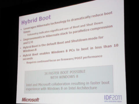
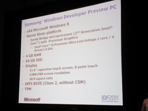
The reason I got over missing the Oprah moment is because the following day Microsoft's people came up to San Francisco and presented several sessions on Windows 8. And they brought one of those Oprah tablets with them. As we now know more than 3 months after the fact, the tablets were Samsung Windows tablets installed with 4GB of RAM and 64GB of SSD. One of the big goals with Windows 8 is to address boot time, and during the demo the tablet was shown cold booting into the login prompt in about 2 seconds. Not bad. Boot time is something Microsoft is finally taking seriously. A couple of other slides highlighted some of the major design points of Windows 8, one of them being the Hybrid Boot which improves hibernate and resume, and the other being the tickless kernel.
Tickless kernel
One of the fundamental enhancements in Windows 8 is the elimination of the periodic timer tick, an artifact from MS-DOS back when it was an 18 Hz tick and the only way to accurately measure time. The tick frequency was a result taking the 1.193 MHz clock frequency (which as I describe a long time ago was based on 1/4 of the 4.77 MHz frequency of the original IBM PC) and dividing it by 65536. Every 65536 counts of the 1.193 MHz clock a timer interrupt would fire. In Windows 95 the rate was increase by a factor of 4 to 72 Hz, and that's roughly the timer tick you see today which gives functions like GetTickCount() their 15 millisecond granularity.
Something that the Linux community realized years ago is that periodic timer ticks (which can typically be 100 Hz, 250Hz or even 1000 Hz on Linux) don't leave a lot of cycles for sleep. If the computer is idling and the processor tries to go into a sleep state, within a millisecond you might get a timer interrupt and need to wake up. At something like 1.6 GHz, millisecond timer ticks barely leave a million cycles to do useful work and go into sleep for it to matter to power.
So in about the Linux 2.6.23 kernel (I believe, .23? .24?) they introduced the concept of a "tickless kernel", replacing the periodic timer interrupt with interrupts programmed to go off when needed. It turns out timer interrupts are not just bad for power consumption, they are bad for virtualization. Almost every virtual product out there including VMware has issues with guest OS clock drift, caused by the latency it takes a virtual machine hypervisor to pass on a timer tick to the guest OS. Sometimes this latency is long enough that another real timer tick already goes off and makes the first tick not get handled, which causes the guest OS to lose time. Or, the guest OS tries to be clever and realizes it is losing ticks and overcompensates, resulting in guest OS time creeping forward. I have seen this effect first hand going way back to trying emulate accurate 200 Hz timer ticks on the emulated Atari ST. VMware's support documentations recommends reducing the timer tick frequency inside the guest OS, like say from 1000 Hz to 100 Hz, to reduce clock drift. But the better fix is to just not have unnecessary timer interrupts in the first place.
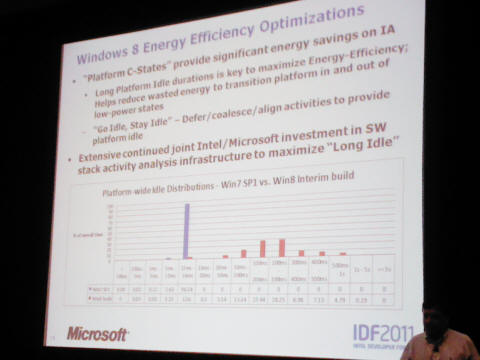
As you can sort of see in the screen capture above, Microsoft has found that the average sleep period now on Windows 8 goes from the the steady 15ms in Windows XP and Windows 7 (that's the solid blue bar in the graph) to a more bell curve distribution centered at around 200 to 300 milliseconds. In other words, your laptop, your tablet, your computer will idle in sleep state up to 10 times longer with Windows 8 than Windows 7, saving significant amounts of power.
But even more importantly for those of us who run Windows in a virtualized environment, fewer cycles will be lost simulating unnecessary timer interrupts, fewer VM exit events, less clock drift.
A tickless Windows kernel is a long overdue and necessary enhancement.
Visual Studio 2011
The Windows 8 Preview also comes bundled with Visual Studio 2011 Preview all pre-loaded and ready to run. You know, Microsoft should just take a hint from Linux and Mac OS and always just always include developer tools bundled with the OS disc. There is certainly plenty of room on the DVD at least for a minimal command line "tree copy" install. And as with previous releases of Visual Studio 98, 2005, 2010, etc. it is possible to easily extract the compiler tools, headers, and libraries into a standalone tree and be used from the command line, which is how I use Visual Studio 99.9% of the time.
Compiling Bochs 2.5 with both Visual Studio 2010 and the 2011 Preview does show minor code size and performance improvements, giving me a few extra MIPS of simulation performance over 2010.
One of the things to watch out for if comparing VS2011 code against VC2010 code is that by default now the VS2011 compiler emits SSE2 code for 32-bit x86 targets. So when you are comparing VC2011 against VS2010 or VS98 or what have you, make sure to throw the /arch:SSE2 switch with the older compiler.
Windows on EC2
Something most people don't know is that when I left Intel last year and took the summer off I then returned to working full time at Amazon's headquarters in downtown Seattle. I am going to give a very shameless plug for a product I worked on, as it is very much one of the very cool products of 2011 that qualifies for the "Faster" category.
I was intrigued by Amazon EC2 (which stands for Elastic Cloud Computing) because it delivers some of the vision I described in my 2007 posting (Part 7) where I said the next "killer app" would be for someone like Google to host virtual machines in the web. The scenario I gave was when travelling on vacation or business and to have a reliable Windows environment accessible. Well, that killer app is now called by the buzzword "the cloud", and unknown to me in 2007, Amazon was already building the foundation for such a cloud hosting service, which is EC2.
I was already a paying customer of EC2 prior to leaving Intel and experimented with it in depth during my travels to ISCA in France and around Europe that summer. I launched some Windows virtual machines (which are called "instances" in EC2 terminology) in Amazon's Virginia datacenter and accessed them from Europe. I used my inexpensive Atom netbook to connect via wi-fi and Remote Desktop into those instances in Virginia.
I was worried about latency. For example moving the mouse on the netbook requires the Remote Desktop protocol to transmit that movement across the Atlantic to the instance running in the datacenter. The Windows instance then has to react to the mouse movement, move the desktop mouse, and render that updated mouse position to the virtual screen. That is then transmitted back across the Atlantic and rendered locally on the netbook. This is the kind of network delay that online gamers worry about, since the tiniest bit of delay can put your player at a disadvantage, and a lagging mouse cursor is equally annoying. But the mouse latency was really not bad. In hindsight, the hop across the Atlantic from Virginia to northern France is not much further than the hop from Virginia to Seattle, so latency should have been comparable to what I saw in Seattle, as it was.
But one thing that irked me early in 2010 is that at the time Windows was sort of a second class citizen on EC2, with most of the features and attention being focused to Linux instances. For one thing, Amazon's Windows offering was limited to Windows 2003 and 2008 (the XP and Vista server versions of Windows). Missing was Windows 2008 R2 (the Windows 7 based server), performance was erratic on different instances, and worse, I experienced that severe clock drift problem that I describe above. Using Windows on EC2 was disappointing, so I hired into Amazon with my list of gripes about Windows and set about to help fix them along with the team of people working the Windows and Cluster products.
Fast forward to September of this year, in fact just days after the IDF and MS BUILD conferences, and the end result of months of sleepless nights and hair pulling launched. Windows 2008 R2 (SP1 even!) was released to EC2's Cluster Computer instance types, knows as cc1.4xlarge and cg1.4xlarge. These are heavy duty instance types based on 2.93 GHz 8-core 16-thread Intel Xeon boxes with tons of memory and 10 gigabit Ethernet; the kind of instances that make great Windows workstations, with the difference that cg1.4xlarge also includes a pair of nVidia cards allowing you to run Cuda applications in the cloud. The end product has no clock drift, and near bare metal performance of network, memory, and Windows system calls.
There was an even cooler announcement Amazon had up its sleeve that we had to keep mum until the Supercomputing SC11 conference here in Seattle last month. Amazon announced an even beefier Windows product called cc2.8xlarge, featuring a 2.6 GHz 16-core 32-thread instance delivering almost triple the performance of cc1.4xlarge:
EC2 instance performance is measured in units called ECUs (Elastic Computer Units), which are roughly equivalent to units of 1 GHz performance on an Intel Core 2. The m1.xlarge instance type for example which is a 2.0 GHz 4-core instance type is rated ECU=8. cc1.4xlarge rates ECU=33.5, while cc2.8xlarge rates a whopping ECU=88. It is quite the beast and not the hardware you can walk down to Fry's and build at home. And if you had such a machine this is an example of what Windows Task Manager would show you (as shown in this cc2.8xlarge screen shot):
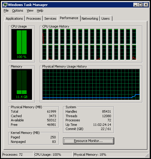
You can buy time on a cc2.8xlarge instance for all of $2.97/hour, which includes a fully activated copy of Windows 2008 R2 Datacenter Server, a terabyte of free local disk storage, and over 60 gigabytes of physical RAM. I went to college in the 1980's when a typical Atari ST or IBM AT had 1 to 4 megabytes of RAM. Imagine how much easier computer science problems would be to solve and passwords would be to crack if we had all had 60 gigabytes of RAM in our machines, grrr! About a thousand of these cc2.8xlarge beasts were clustered together prior to SC11 to do a Top 500 run, resulting in a virtual supercomputer that ranked #42 on the most recent Top 500 list of world's fastest supercomputers:
https://www.readwriteweb.com/cloud/2011/11/amazon-ec2-now-42-supercompute.php
In other words, for about 3 grand per hour you too can host your own Top 500 supercomputer in the cloud. I don't do that, but I do use EC2 instance to surf the web when I travel, because even if you remote in from France or Australia, your web surfing takes place in the geographic location of the datacenter you launched in (e.g. Virginia or Oregon or Tokyo), giving you one workaround to watching Hulu and Netflix videos from abroad. I also realized that web surfing is also much faster in the cloud, since the Firefox or Chrome you run in the cloud has very beefy (on the order of hundreds of megabit) pipes to the Internet. Again, great for surfing from a remote location. This is also the basis of the way that Kindle Fire browsers are able to surf the web faster than other tablets.
Windows 7 Thin PC Edition
Not to be forgotten, Windows 7 is still the main operating system most of us are going to use until at least Windows 8 comes out. On July 1 2011 Microsoft did a somewhat stealthy release of one final new Windows 7 edition called Windows 7 Thin PC Edition. As an MSDN subscriber I was able to download the ISO image, which is otherwise only made available to OEMs and not for public sale.
Thin PC Edition is advertized as a stripped down, almost crippled, version of Windows 7 suitable for running on thin clients, i.e. very weak computers that you mainly use to remote into other machines. Microsoft claims that you can't install many other apps on it, and really should use it in embedded devices and old computers.
Well, this advice turns out to be nonsense. Windows 7 Thin PC Edition is the Windows release that most people would crave for. It is the only version of Windows 7 which can install to the hard drive using a footprint of under 3 gigabytes. I confirmed this by installing Thin PC Edition to my old ASUS EEE netbook, which comes with only 512MB of RAM and a 4GB SSD. Even Windows 7 Home Edition can't fit on this machine, yet Thin PC Edition easily did install and boot just fine. I also found, as other people did, that you can install Office and Firefox and other applications just fine.
Thin PC Edition also runs great inside of a simulator like Bochs. Whereas Windows XP needs about 4 billion x86 instructions to boot, Windows Vista bloated that to about 25 billion, and even Windows 7 normally needs about 20 billion instructions to completely boot up to the desktop. Windows 7 Thin PC Edition is booted at the desktop in only 12 billion instructions, or just under 2 minutes of wall clock time of simulation. It's great if you want to do x86 instruction analysis on modern Windows 7 workloads without tracing through something bloated like Windows 7 Ultimate.
Bottom line: it truly is smaller, thinner, faster than regular Windows 7, and is comparable in disk footprint to Windows XP SP2.
Microsoft could have easily marketed Thin PC Edition an upgrade to Windows XP user holding out from upgrading to Windows 7 because they believe their performance will be slow. Why they are only making it an OEM product is baffling. But if you can get your hands on it, you'll love it!